
Challenges Associated With PCB Manufacturing Assembly
PCB Manufacturing Assembly
The PCB manufacturing assembly process is complex and requires strict protocols and inspection procedures. In addition, the industry is constantly changing, bringing with it new challenges like component shortages and new materials and technologies. However, these new challenges also create opportunities for companies that are willing to adapt and embrace the change.
Most PCB problems arise from issues during the fabrication process, including soldering defects such as solder bridging (when two areas that should be electrically isolated are connected), cold solder joints (when solder is not given enough time to melt and form a solid bond between different surfaces), and acid traps (when copper ions seep into the metallization and damage the circuit board). Soldering defects can be minimized by performing rigorous design for manufacturability analysis and following detailed fabrication processes.
One of the biggest challenges facing PCB manufacturers today is a lack of raw material supplies. The pandemic has highlighted the fragility of global logistics and supply chains, resulting in shipping delays, surging prices, and shortages of many of the essential components used to produce PCBs. Insufficient availability of raw materials can increase the cost of a finished product, cause production delays, and negatively impact customer satisfaction.
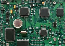
Challenges Associated With PCB Manufacturing Assembly
Another common problem in pcb manufacturing assembly is insufficient space to accommodate miniature components. The shrinking size of PCB components is a driving force behind the need for ultra-precise placement accuracy in order to maintain acceptable tolerances. Even minor placement inaccuracies can disrupt signal flow and reduce reliability. Miniature parts like 01005-size resistors and capacitors measure just 0.4 x 0.2 mm, meaning that machines must place them with a high degree of precision to avoid problems.
A third issue in PCB assembly is the difficulty of reworking and repairs on densely packed, miniature assemblies. Due to their small size, these assemblies are often difficult to reach or move without damaging the component or the board itself. Trying to fix or replace these highly compact components can be expensive and time-consuming.
The final challenge in PCB assembly is ensuring that all required testing is conducted. This includes electromagnetic interference testing (EMI) for assemblies that contain mixed-signal or RF components, and functionality and performance tests. Failure to conduct these tests can lead to costly recalls and brand damage. Environmental considerations also play an important role in modern PCB assembly. The industry has embraced lead-free soldering to comply with regulations like RoHS (Restriction of Hazardous Substances), ensuring that electronic products are environmentally friendly. Manufacturers also focus on waste reduction, energy efficiency, and sustainable material sourcing as part of their commitment to green manufacturing practices.
Another important step in the PCB assembly process is completing accurate silkscreen markings such as reference designators and polarity indicators. These labels help test technicians find the right spot on the board to perform tests, rework, and repair. Inaccurate or missing silkscreen markings can make it extremely challenging for these workers to complete their jobs. This can significantly delay the testing and rework processes, increasing assembly costs and reducing quality.