
How PCBs Are Produced and Recycled
PCBs Are Produced and Recycled
Computer circuit boards are essential components of electronic devices like tablets, smartphones, and computers. They contain precious metals and minerals that can be extracted and repurposed through recycling, reducing the need to mine and conserve natural resources. However, the process of recycling PCBs is complex and involves shredding and separating the materials using specialized equipment. This approach is resource-intensive and can pollute the environment, but new technologies may change this. Researchers from the University of Washington (UW) are developing a solution that can help reduce the environmental impact of e-waste and make it easier to recycle circuit boards.
A pcba circuit board is an essential component of any electronic device, connecting all the necessary components to each other through conductive pathways etched into laminated copper sheets. These paths, known as traces, facilitate the transfer of current between different parts and allow for functions like power making, signal amplification, attenuation, modulation, and coding.
The process of producing a circuit board starts with a blueprint, or schematic, which is the foundation of a new device’s design. It lays the groundwork for all subsequent manufacturing steps and significantly impacts production outcomes. Engineers can use schematic capture tools to speed up this process and ensure seamless synchronization between schematic and layout files.
After the schematic is completed, it’s time to insert the components into the layout. This is a crucial step that can be done manually or through automated processes using machines with computerized vision systems. These machines can identify components that are smaller than a grain of rice and solder them into place with precision accuracy.
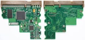
How PCBs Are Produced and Recycled
Once the components are in place, it’s time to test the circuit board. This can be accomplished through various methods, including visual inspections and electrical testing. In-process testing can also be conducted during production to identify potential problems before they become major issues that could affect the product’s quality or functionality.
Finally, it’s time to add labels and identifiers to the circuit board to facilitate assembly and repair. This is a crucial step for PCBAs, as it helps to prevent misidentification of components and improve overall productivity. A good pcba manufacturer will provide comprehensive design engineering, prototyping, and manufacturing services to get products to market faster and with less risk.
A pcba manufacturer should offer rapid turnaround times and a high level of customer service, as well as a Design for Manufacturability (DFM) report. This document will help avoid costly mistakes during the design process and save time and money later on in production. It can also recommend changes to the original design that will increase the product’s quality, reliability, and cost-effectiveness. This is a crucial step in ensuring that the final product meets all requirements and specifications. A reputable and experienced manufacturer will also be able to guarantee high-quality, functional testing, and delivery of a complete PCBA on time. This will help customers to meet their project deadlines and keep their businesses running smoothly.
In summary, PCBs are indispensable in RF applications, providing the platform for designing and implementing high-performance RF systems across various industries. Their versatility, compactness, and signal integrity make them essential components in modern RF technology.