
How do you address issues related to PCB warpage during assembly?
address issues related to PCB warpage during assembly
In the realm of PC board assembly, dealing with issues related to PCB warpage stands as a critical challenge that manufacturers must overcome to ensure the integrity, reliability, and functionality of electronic devices. PCB warpage, characterized by bending or deformation of the board, can lead to misalignment of components, stress on solder joints, and compromised electrical connections, ultimately impacting the performance and longevity of electronic devices. In this article, we explore the strategies and techniques for addressing issues related to PCB warpage during assembly and ensuring high-quality soldering results.
One of the primary strategies for addressing PCB warpage during assembly is selecting the appropriate PCB materials and thicknesses that offer dimensional stability and mechanical rigidity. High-quality laminates with low coefficients of thermal expansion (CTE), such as FR-4 epoxy resin, help minimize the risk of warping and deformation during temperature fluctuations encountered during soldering and assembly. Additionally, thicker PCBs provide greater structural integrity and resistance to warping, especially for larger PCBs or those with heavy components.
Furthermore, optimizing the design and layout of pc board assembly to minimize thermal gradients and mechanical stress during assembly is essential for addressing PCB warpage. By evenly distributing components and traces across the PCB surface and avoiding concentrated heat sources, designers can reduce the risk of thermal distortion and warping during soldering. Additionally, ensuring proper spacing between components and clearance around high-heat components helps minimize localized heating and cooling, reducing the risk of thermal stress and warping during assembly.
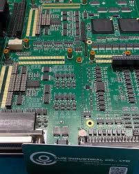
How do you address issues related to PCB warpage during assembly?
Moreover, implementing proper handling and support techniques during assembly is essential for addressing PCB warpage. Handling PCBs with care and avoiding excessive bending or flexing helps maintain their flatness and integrity throughout the assembly process. Additionally, providing adequate support and fixation for PCBs during soldering and cooling stages helps prevent sagging or deformation under the weight of components or thermal stress, minimizing the risk of warping and ensuring consistent soldering results.
In addition to process optimization, implementing proper soldering techniques and process parameters is essential for addressing PCB warpage during assembly. By controlling the temperature, heating rate, and cooling rate during reflow soldering, manufacturers can minimize thermal shock and mechanical stress on the PCB, reducing the risk of warping and deformation. Additionally, using solder pastes with appropriate rheological properties and flux formulations helps ensure uniform solder wetting and adhesion, minimizing the risk of component misalignment and warping during reflow soldering.
Furthermore, implementing proper cooling and curing processes after assembly is essential for addressing PCB warpage. By gradually cooling PCB assemblies to room temperature in a controlled manner, manufacturers can minimize thermal gradients and mechanical stress, reducing the risk of warping and deformation. Additionally, curing adhesives and conformal coatings at the appropriate temperature and humidity levels ensures proper bonding and adhesion without inducing warping or distortion in PCB assemblies.
Moreover, implementing comprehensive inspection and quality control measures is essential for detecting and addressing PCB warpage issues during assembly. Visual inspection, automated optical inspection (AOI), and X-ray inspection techniques can be used to identify warpage defects and abnormalities in PCB assemblies, enabling manufacturers to take corrective action and ensure compliance with quality standards. Additionally, implementing mechanical testing techniques such as shear testing, pull testing, and bend testing can assess the mechanical strength and integrity of solder joints and evaluate the resilience of PCB assemblies to mechanical stress and warpage.