
How do you prevent delamination in hdi pcb fabrication?
prevent delamination in hdi pcb fabrication
Preventing delamination in high-density interconnect (HDI) printed circuit board (PCB) fabrication is crucial for ensuring the reliability and performance of electronic devices. Delamination occurs when the layers of a PCB separate or detach from each other, compromising the structural integrity and electrical properties of the board. Several factors contribute to delamination, including materials, manufacturing processes, design considerations, and environmental conditions. Implementing effective preventive measures is essential to mitigate the risk of delamination in HDI PCB fabrication.
One of the primary causes of delamination is inadequate bonding between layers during the lamination process. Proper surface preparation, including cleaning and roughening, is essential to promote adhesion between substrate layers and ensure a strong bond. Additionally, using high-quality bonding materials, such as epoxy resins or adhesives with appropriate curing properties, helps improve bonding strength and reduce the likelihood of delamination.
Furthermore, controlling the lamination process parameters, such as temperature, pressure, and duration, is critical for preventing delamination in hdi pcb fabrication. The lamination process must be carefully optimized to ensure uniform heating and pressure distribution across the entire PCB stackup. Excessive heat or pressure can cause thermal stress and mechanical deformation, leading to delamination issues. Therefore, maintaining tight control over lamination parameters and following recommended guidelines is essential for achieving reliable lamination results.
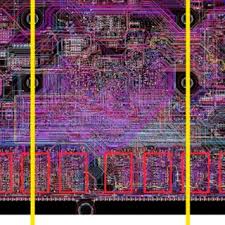
How do you prevent delamination in hdi pcb fabrication?
Moreover, selecting suitable substrate materials with compatible thermal and mechanical properties is essential for preventing delamination in HDI PCB fabrication. Materials with low coefficient of thermal expansion (CTE) and high glass transition temperature (Tg) offer better dimensional stability and resistance to thermal stress, reducing the risk of delamination. Additionally, using materials with low moisture absorption properties helps minimize the effects of moisture-induced delamination, especially in humid or harsh environments.
In addition to materials and manufacturing processes, proper design considerations play a crucial role in preventing delamination in HDI PCB fabrication. Designing PCBs with balanced layer stackups, uniform copper distribution, and controlled aspect ratios helps reduce stress concentration and minimize the risk of delamination. Avoiding sharp corners, abrupt changes in trace width, and excessive copper thickness variation also helps improve the mechanical stability and reliability of the PCB.
Furthermore, implementing thorough testing and quality control measures is essential for detecting and preventing delamination issues in HDI PCB fabrication. Non-destructive testing techniques, such as thermal imaging, acoustic microscopy, and bond strength testing, can identify potential delamination defects before they become critical issues. Additionally, conducting reliability testing, such as thermal cycling, humidity testing, and thermal shock testing, helps assess the long-term durability and performance of HDI PCBs under various environmental conditions.
Environmental factors, such as exposure to moisture, temperature fluctuations, and mechanical stress, can exacerbate delamination issues in HDI PCB fabrication. Therefore, implementing proper environmental protection measures, such as conformal coatings, encapsulation, and moisture barrier materials, helps mitigate the effects of environmental factors and prevent delamination. These protective measures create a barrier against moisture ingress, chemical exposure, and mechanical damage, ensuring the long-term reliability and performance of HDI PCBs in diverse operating environments.
In conclusion, preventing delamination in HDI PCB fabrication requires a holistic approach that encompasses materials selection, manufacturing processes optimization, design considerations, testing and quality control measures, and environmental protection strategies. By addressing these factors systematically and proactively, manufacturers can minimize the risk of delamination and ensure the reliability and performance of HDI PCBs in a wide range of electronic applications.