
How to Troubleshoot Issues in Rigid Flex PCB Design
Troubleshoot Issues in Rigid Flex PCB Design
Rigid flex circuits have evolved from an engineering technology into a powerful solution for today’s complex and demanding electronic devices. They offer many advantages, but like other PCB technologies they also pose some challenges. This blog series will help you troubleshoot these issues and ensure your rigid flex pcb supplier is reliable and robust.
Rigid-Flex PCBs are hybrids that combine the stability of standard rigid boards with flexible circuitry, creating a board that can be folded or continuously flexed without damage to the copper layers or the dielectric materials. They are typically made with an outermost insulating layer of Polyimide (PI) that is covered with a solder mask layer and plated with copper, similar to traditional rigid boards. The flexible components are buried within the outer layers, while the copper traces on the surface of the board are connected to the copper pillars through Microvias or laser-drilled holes that are then plated through to make them conductive. The fabrication process can stagger or stack these Microvias to simulate the blind and buried plated through holes found in regular rigid PCBs.
The benefits of using rigid flex include increased reliability, improved durability and reduced assembly costs. The ability to bend reduces the need for connectors, which can be prone to breakage in high-speed or vibration environments, and it frees up space inside the device, allowing it to fit into tight spaces. Rigid flex PCBs can also be used for applications that require an extra level of mechanical flexibility and durability, such as medical imaging equipment or military missile guidance systems.
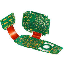
How to Troubleshoot Issues in Rigid Flex PCB Design
Some of the most common issues encountered in rigid flex are caused by conductor stress points, a problem that can cause fractures in the flexible sections of the circuit. These fractures are usually triggered by stacked traces or a solder joint that is too close to the bend point. This issue can be solved by designing the traces so they are not overlapping, and by placing dummy traces in the corners of the rigid area.
Other common rigid flex PCB problems include incorrect bend radius calculations and lack of adequate hole-to-flex spacing. Defining a correct bend radius helps prevent excessive strain on the flex section of the circuit, which can cause it to deteriorate or short. A proper hole-to-flex spacing allows the copper to be properly routed through the flex section, without interfering with the rigid sections and the underlying conductive material.
A rigid flex PCB manufacturer should provide advice on the optimal bend radius for each specific application, as well as the minimum bend diameter for the entire circuit. They should also be able to advise on the best methods for minimizing the risk of defects in the transition zone between the rigid and flex sections. The most effective solutions to these issues include extending the flex coverlay into the rigid region, and adding a bead of flexible epoxy strain relief and flexible epoxy stress relief at the transition area.
Rework involves the identification and rectification of defects or errors in the PCB assembly. This could include addressing issues such as misalignment of components, soldering defects, electrical connectivity issues, or any other anomalies that could compromise the performance or reliability of the PCB.