
What are the most common failure modes for custom pcb?
most common failure modes for custom pcb
Custom printed circuit boards (PCBs) serve as the backbone of electronic devices, facilitating connectivity and functionality. However, like any complex system, custom PCBs are susceptible to various failure modes that can compromise their performance and reliability. Understanding the most common failure modes is essential for mitigating risks and ensuring the longevity of electronic systems.
One of the most common failure modes for custom PCBs is solder joint failure. Solder joints connect electronic components to the PCB, forming electrical and mechanical bonds. Factors such as thermal cycling, mechanical stress, and vibration can weaken solder joints over time, leading to cracks or fractures. Cold solder joints, insufficient solder, or improper soldering techniques during assembly can also contribute to solder joint failures. These failures can result in intermittent connections, open circuits, or short circuits, causing malfunctions or complete system failures.
Another prevalent failure mode in custom pcb is due to electrical overstress (EOS) or electrostatic discharge (ESD). EOS occurs when excessive current or voltage levels exceed the rated specifications of electronic components, causing damage to sensitive components such as integrated circuits (ICs) or transistors. ESD, on the other hand, occurs when static electricity discharges through the PCB, potentially damaging or degrading semiconductor devices. Proper grounding, ESD protection measures, and component selection are critical in mitigating EOS and ESD-related failures.
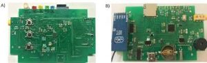
What are the most common failure modes for custom pcb?
Furthermore, environmental factors such as moisture ingress, temperature extremes, and exposure to contaminants can contribute to PCB failures. Moisture ingress can lead to corrosion of conductive traces or components, compromising electrical connections and causing short circuits. Temperature extremes can induce thermal expansion and contraction, stressing the PCB substrate and components, potentially leading to delamination, warping, or component failure. Contaminants such as dust, dirt, or chemical residues can also degrade PCB performance over time, affecting signal integrity or causing electrical shorts.
Mechanical stress is another significant contributor to PCB failures, especially in applications subject to vibration, shock, or mechanical strain. Excessive mechanical stress can lead to mechanical damage, such as cracks in the PCB substrate or fractured components. Inadequate mounting or insufficient support for heavy components can exacerbate mechanical stress, increasing the risk of mechanical failure. Proper mechanical design, including adequate reinforcement, mounting techniques, and vibration isolation, is essential for mitigating mechanical stress-related failures.
Furthermore, design flaws or manufacturing defects can contribute to PCB failures. Design errors such as inadequate clearance between traces, improper component placement, or inadequate thermal management can compromise PCB performance and reliability. Manufacturing defects such as missing or misaligned components, solder bridging, or contamination during assembly can also lead to PCB failures. Comprehensive design validation, testing, and quality assurance processes are necessary to identify and rectify design and manufacturing issues before deployment.
In conclusion, custom PCBs are susceptible to various failure modes that can compromise their performance and reliability. Solder joint failure, electrical overstress, environmental factors, mechanical stress, and design/manufacturing defects are among the most common causes of PCB failures. Mitigating these risks requires careful design considerations, proper assembly techniques, environmental protection measures, and thorough testing and validation processes. By addressing these factors, PCB designers and manufacturers can create custom PCBs that deliver optimal performance and reliability in diverse applications.